TMS320F280x checks below four pins at the reset to decide the booting mode.
| Boot mode | GPIO18 SPICLKA SCITXB |
GPIO29 SCITXDA |
GPIO34 |
| Jump to Flash 0x3F 7FF6 | 1 | 1 | 1 |
| Call SCI-A boot
loader (RAM boot) |
1 | 1 | 0 |
| Call SPI-A boot loader | 1 | 0 | 1 |
| Call I2C-A boot loader | 1 | 0 | 0 |
| Call eCAN-A boot loader | 0 | 1 | 1 |
| Jump to M0 SARAM 0x00 0000 | 0 | 1 | 0 |
| Jump to OPT | 0 | 0 | 1 |
| Parallel GPIO Loader | 0 | 0 | 0 |
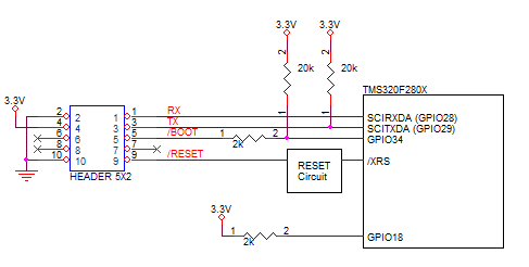
easyDSP uses two kinds boot mode. 'SCI-A' for RAM booting, 'Jump to Flash' for flashrom booting (yellow part in above table). Therefore, fix GPIO18, GPIO29 to '1'. And connect GPIO34 to /BOOT pin of easyDSP, as shown in below connection.

- power pin (#4) of
easyDSP 5x2 header should be connected to 3.3V
- TX/RX pins are directly connected to
MCU pins
- In case there is a reset IC between
easyDSP /RESET and MCU /XRS, it should transfer easyDSP /RESET signal to MCU /XRS
within 0.5sec
- In case you insert buffer IC between easyDSP
header and MCU, place buffer IC directly to easyDSP header so that all resistors
can be connected to directly MCU
- /RESET pin is connected to reset
generation circuit of MCU
board
(Time duration of /RESET pin is around 500msec)
- In case you use pull-up resistor to each pin, the value
of pull-up resistor should be higher than a few kilo ohm since there is 100Ω
series resistor inside easyDSP pod
- Refer to
here
for BOOT pin
operation mode.
Please be careful when you use
your own pull-up or pull-down resistor on the easyDSP signal pins. Please use
appropriate filter circuit to your reset generation circuit to prevent
unintentional reset generation.